Z80 Single-board Computer
A single board Z80 computer of my own design. 32K ROM, 64K RAM running at 4Mhz.
I have long been intrigued by the idea of creating a simple microprocessor system, and I recently had the chance to turn this interest into a reality. I designed a basic Z80 single-board computer, which serves as an initial step towards a potentially more complex system in the future. While the project was not particularly challenging, it provided me with valuable experience and I am pleased with the end result. I am excited to share my progress and insights with others who may be interested in pursuing similar projects.
Design Requirements
To ensure that I maximized the software potential of the system while minimizing the hardware complexity and cost, I established several design requirements before starting to design the microprocessor system. These requirements were as follows:
Minimum PCB size: To save on cost and physical space, I challenged myself to design a 10cm by 10cm board. At this size, JLCPCB will make the PCB for $7 for 5.
64K RAM: As the Z80 can access a maximum of 64k directly, I wanted to provide the system with as much memory as possible without getting too complex with memory paging.
32K ROM and ZIF Socket: To make the ROM easily removable and installable, I decided to use a ZIF socket. I chose a ROM size of 32K as it maps extremely easily into the Z80's address space. However, to utilize the full 64K RAM, the ROM will have to be paged out by the system software.
9600 Baud Serial: As the microprocessor system does not include a video output circuit, its output must be accessed through a different interface. I have configured the system to output its data through a serial interface at a rate of 9600 baud. This interface is designed to use TTL voltage levels, which are suitable for my purposes.
Keyboard Interface: Although not strictly necessary, I wanted to support some kind of keyboard. Preferably something simple to implement but still reasonably accessible.
IO and Expansion Header: To enhance the capabilities of the system and enable interfacing with external devices, I included some outputs and an expansion header.
Selection of Components
The selection of components was largely decided by what I had in my collection and their compatibility with the Z80.
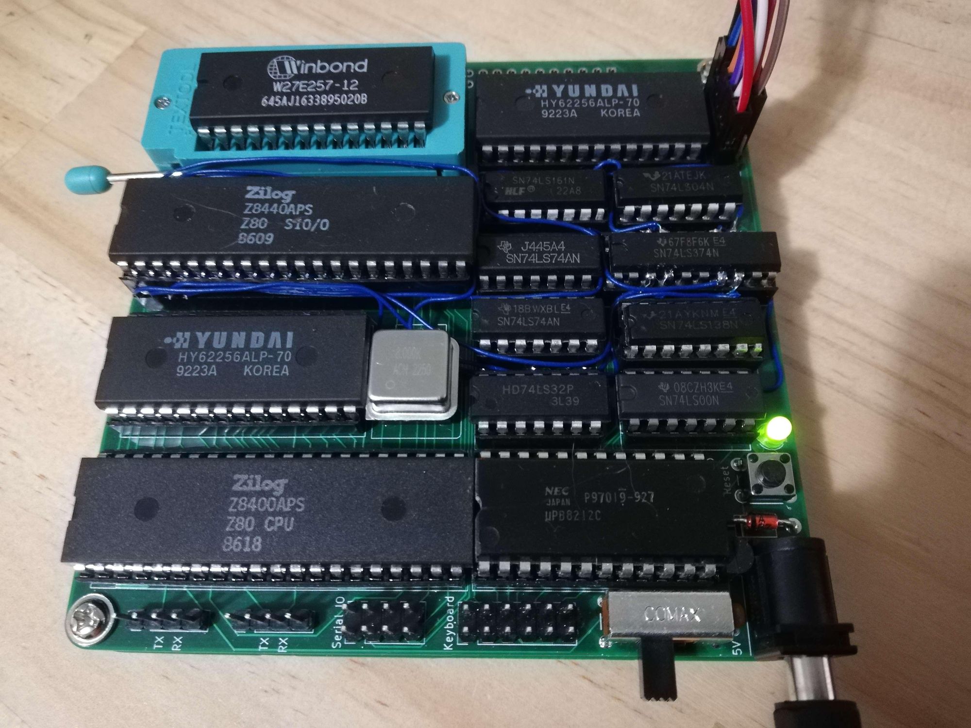
Microprocessor (Z80): I selected the Z80 because I happen to have several in my collection and its 8-bit architecture makes designing the PCB simpler.
Serial/UART (Z8440 SIO): I was initially reluctant to use the Z80 SIO chip because of its large footprint, I would have preferred to use the smaller Intel 8251. Unfortunately, I didn't have any in my collection so Z80 SIO was selected.
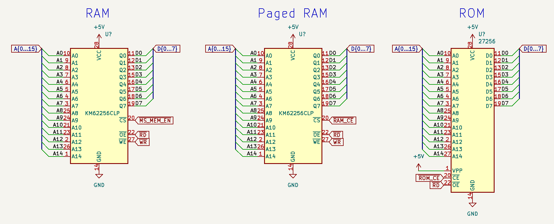
Static RAM (62256): To keep the design simple, I used two generic 62256 static RAM chips to provide the 64K of RAM.
32K ROM (W27E257): While any generic 2732 ROM chip would have worked, I found the Winbond W27E257 electrically erasable 32K ROM chip to be more convenient than UV erasable ROMs.
Keyboard (Intel 8212): The Intel 8212 input/output port is a simple chip that is well-suited for use as a parallel keyboard interface, it has a built-in interrupt line that is triggered whenever data is latched into the chip. The idea to use the 8212 came from a Panasonic system I was repairing at the time.
IO: Due to the limited space on the PCB, the system includes only a single 8-bit parallel output provided by a 74LS374 chip. However, if additional IO is required, the keyboard interface and serial control lines can also be used.
System Design
In developing my first microprocessor system, I sought to strike a balance between simplicity and versatility. With a focus on creating a platform that could support software development, I endeavored to create a design that would be accessible to those just starting out in microprocessor design, like myself. The complete schematics can be seen in the picture below and on my GitHub.
In the following sections, I will explain the most significant aspects of this design and how they interface together.
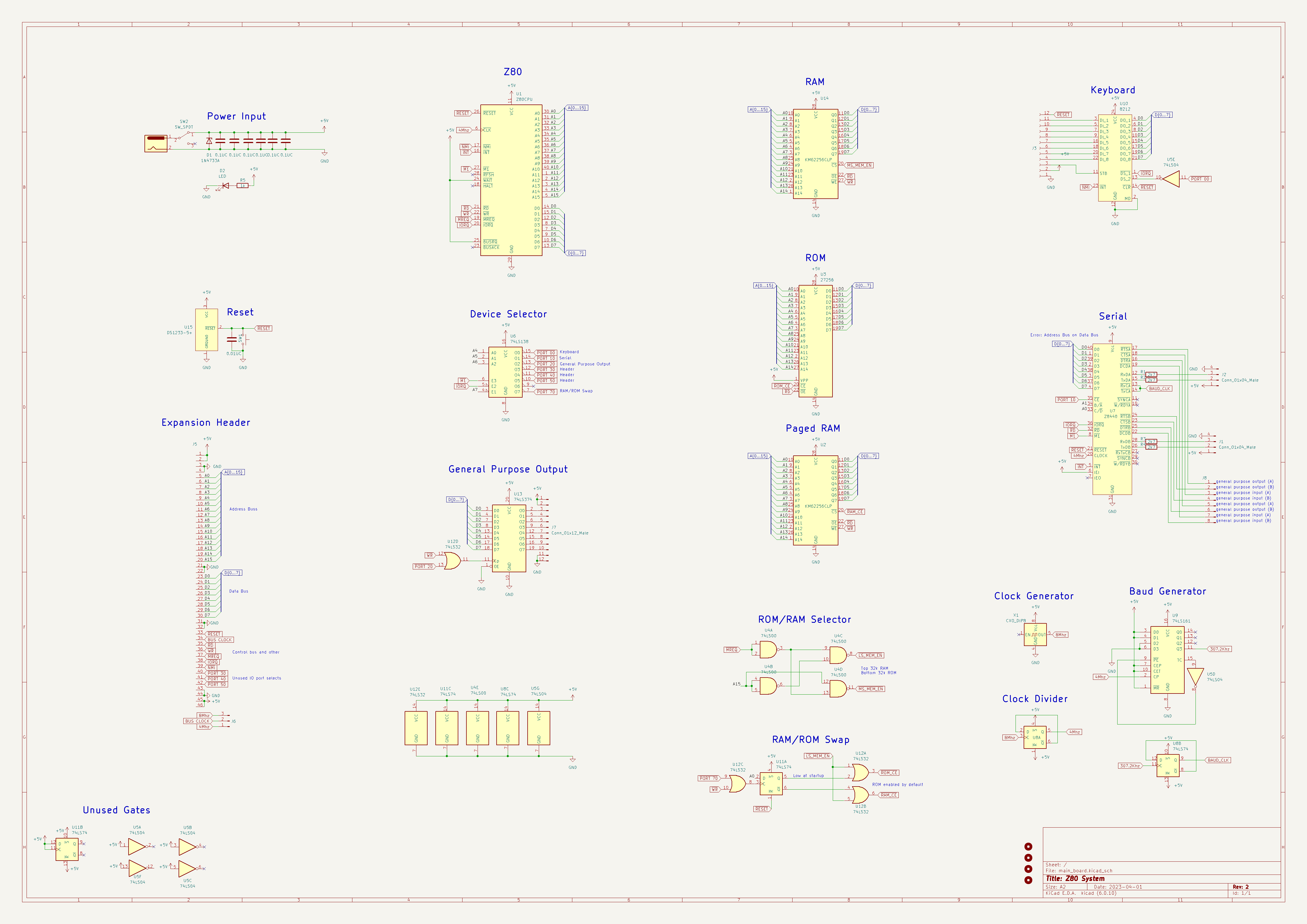
Zilog Z80
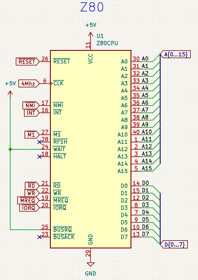
At the heart of the system sits the Zilog Z80 running at 4MHz. The Z80 has a 16-bit address bus and an 8-bit data bus. The internal architecture of the Z80 includes a set of general-purpose registers, an arithmetic and logic unit (ALU), a program counter (PC), and several other control and status registers.
I am not going to go into detail about each pin but the ones that are most significant to us are:
- RD (Read): This signal indicates that the processor is reading data from memory or an I/O device. When RD is asserted, the data from the addressed location is put onto the data bus for the processor to read.
- WR (Write): This signal indicates that the processor is writing data to memory or an I/O device. When WR is asserted, the data on the data bus is written to the addressed location.
- MREQ (Memory Request): This signal is used to indicate that the processor is requesting data from memory or sending data to memory. When MREQ is asserted, the memory or the memory controller responds to the address on the address bus.
- IORQ (I/O Request): This signal is used to indicate that the processor is performing an I/O operation. When IORQ is asserted, the I/O device or controller responds to the address on the address bus.
System Clock
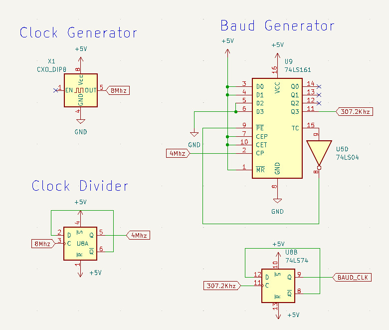
This system requires two clock signals to work correctly. 4MHz for the Z80 and 153.6KHz for the SIO serial chip. This system uses an 8Mhz oscillator which is divided by 2 to produce 4MHz for the Z80, it is then divided by 26 to produce a frequency of 153.6KHz. It so happens that 153.6KHz is 16 times our desired baud rate of 9600.
Device Selector
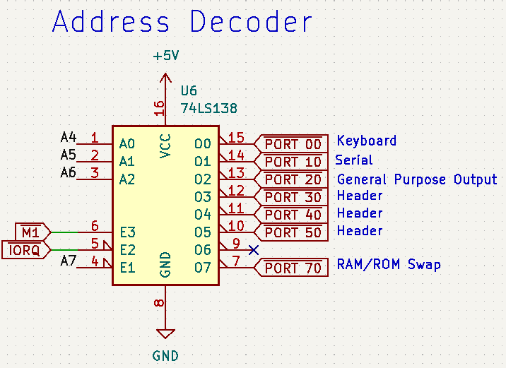
The IO Address Decoder is an essential component that facilitates the selection and activation of specific I/O devices during an I/O Request. The decoder is connected to the address bus of the microprocessor and serves as a map between a single address or address range and an individual I/O device.
By using the IO Address Decoder, specific I/O devices can be selected and enabled during an IO Request. The decoder maps a single address or address range to a single individual I/O device, allowing for easy access to its associated sub-devices or registers. In this system, the 74LS138, 3-to-8 decoder, is used to select a single I/O device at a time using the address lines A4-A7. This allows A0-A6 to be used for the selection of specific sub-devices or registers within a single port range, providing greater flexibility and functionality to the system.
One important note about the Z80 I/O operations is the use of the address lines A8-A15 requires several more instructions and requires a larger time to execute. It's recommended that I/O devices are mapped to the low 8-bit of the address bus.
General Purpose Output
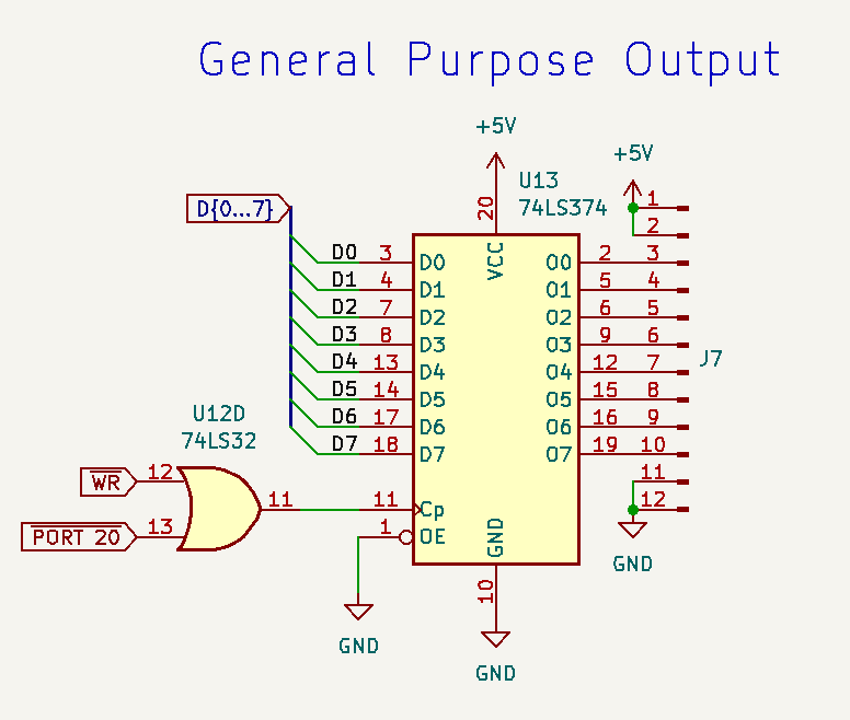
One of the simpler I/O devices in this system is an 8-bit general-purpose output. A single byte is latched into the 74LS374, octal latch, whenever WR and PORT 20 are both low. PORT 20 is low during an I/O request to the address 20h to 2Fh.
Because the 74LS374 lacks any clear or pre-set pins whenever the system is powered up the output of the 74LS374 is random. So the system should set the output to a known state early in the system startup.
As the 74LS374 is only capable of handling a small output current it should only be used to drive TTL devices. Led lights should be driven by a dedicated driver such as the 74HC541.
Parallel Keyboard Interface
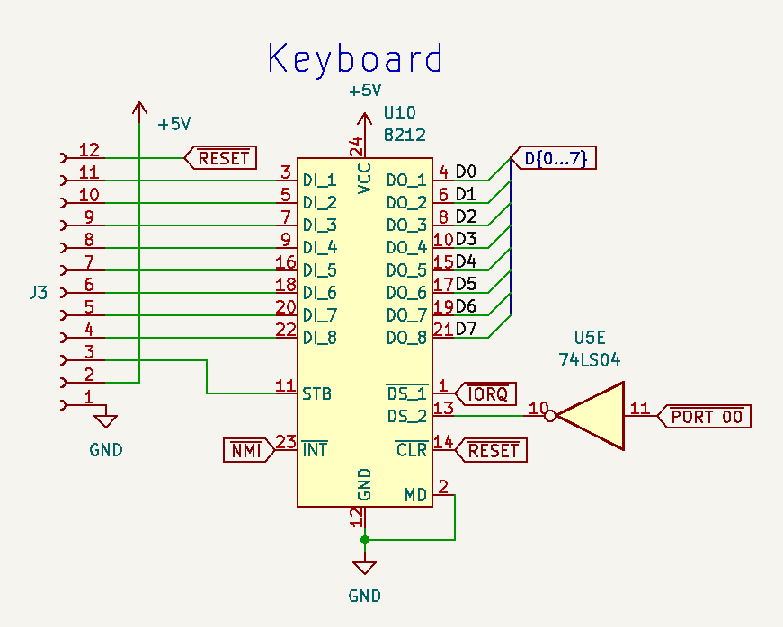
The keyboard interface is provided by the intel 8212, 8-bit input/output port. This chip allows an external device such as a parallel keyboard to latch data into the chip's internal flip-flops and create an interrupt to the Z80 informing it that there is new data to be read into the microprocessor.
A nice feature of this chip is that it will not interrupt Z80 again until the current value has been read out. When the system does not care about the keyboard it can simply ignore the first interrupt and no subsequent interrupts will interrupt the microprocessor.
One issue with the above circuit is that there is nothing guarding against the microprocessor attempting to write to the 8212. This is a problem because both the data bus and 8212's output will be active at the same time causing a collision and potentially damaging either device. The reason I did not fix this problem was that there was not sufficient room on the board for an additional OR gate.
Z80 SIO (Serial)
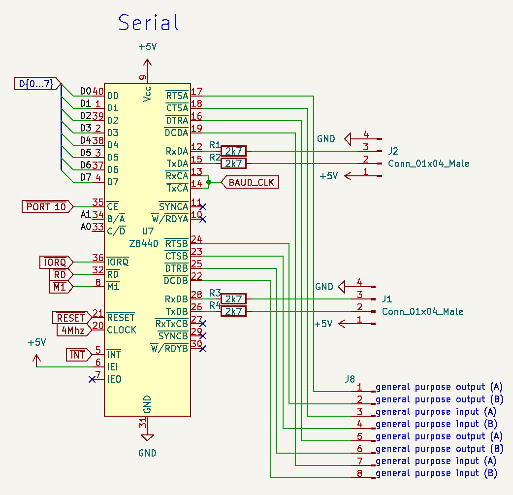
The Z8440 is a versatile dual-channel UART chip (universal asynchronous receiver transmitter) that allows the microprocessor to communicate in several serial protocols. Some of these protocols necessitate independent flow control signals, there are also provided by the Z8440.
However, in my case, I only need the system to support asynchronous serial so those extra flow control lines would have gone unused. Fortunately, the Z8440 allows us to use those unused lines for general-purpose I/O.
The Z8440 has two channels A and B, with each channel having two input modes, Data, and Control. The selection between channels A or B and Data or Control is done on pins 34 and 33 respectively. By connecting these pins to the address bus it becomes possible to address a particular channel and input modes as part of the I/O operation.
Subsequently, the Z8440 chip can be addressed as such:
- 0x10h - Channel A, Data
- 0x11h - Channel A, Control
- 0x12h - Channel B, Data
- 0x13h - Channel B, Control
Memory Address Space
This system has 64K of RAM and 32K of ROM. However, the Z80 can only ever address 64K at a time so when the system starts up the top 32K of memory maps to RAM, and the lower 32K maps to ROM, this is because the ROM contains the system software and must be accessible to the microprocessor at startup.
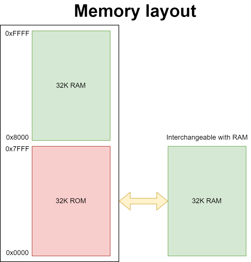
Once the system has started the code in the ROM can copy itself into RAM and jump to it. From then on the system is running from RAM and can safely swap the lower 32K of ROM out for RAM.
ROM/RAM Chip Selection
The selection of ROM and RAM chips is accomplished with the use of two circuits. One is responsible for selecting between the upper 32K or the lower 32K. The second is responsible for the swapping and selection of the lower ROM or RAM.
ROM/RAM Selector
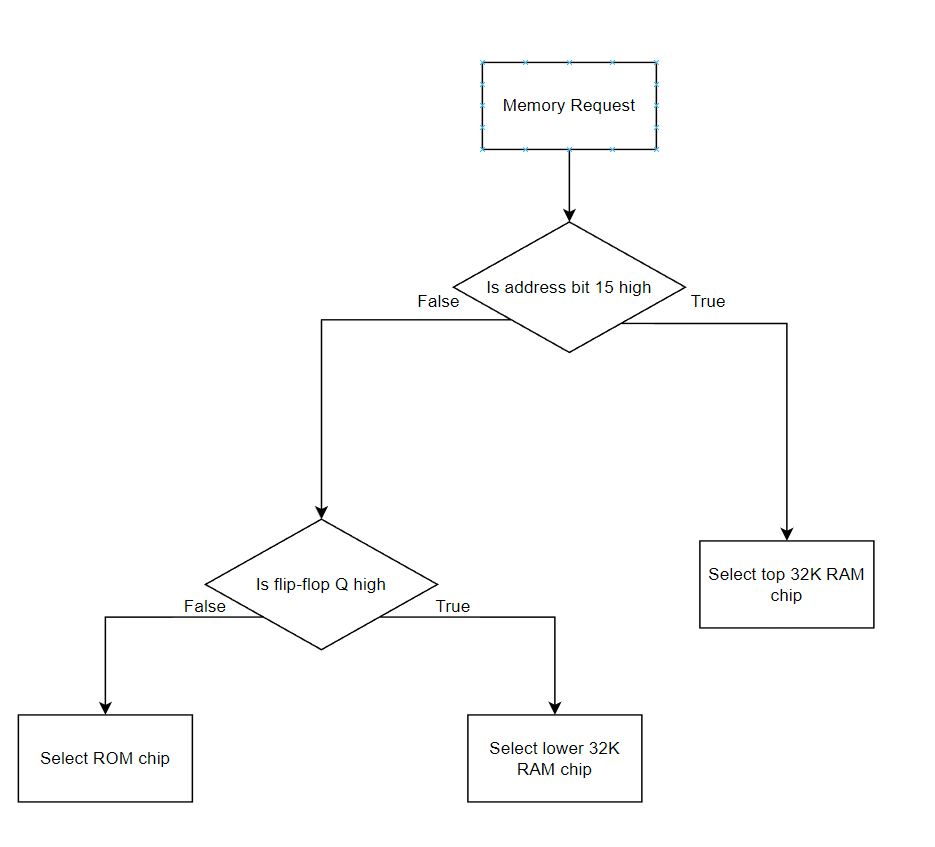
Because the address space is split evenly between ROM and RAM it's a simple matter to map the Z80 address space to the two 32K chips. By examining the most significant address bit, A15, we can determine if we are in the lower or upper address range, LOW being lower 32K and HIGH being upper 32K.
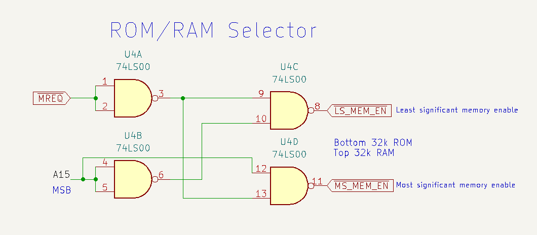
The ROM/RAM Selector circuit will, given that M̅R̅E̅Q̅ (memory request) is LOW, select either the lower or upper RAM/ROM chip.
RAM/ROM Swap
In the case of the lower region of memory, an additional selection has to be made between the ROM or an interchangeable RAM chip. There are two parts to this circuit, a flip-flop that stores the state of the RAM/ROM selection and a couple OR gates to select the appropriate chip.
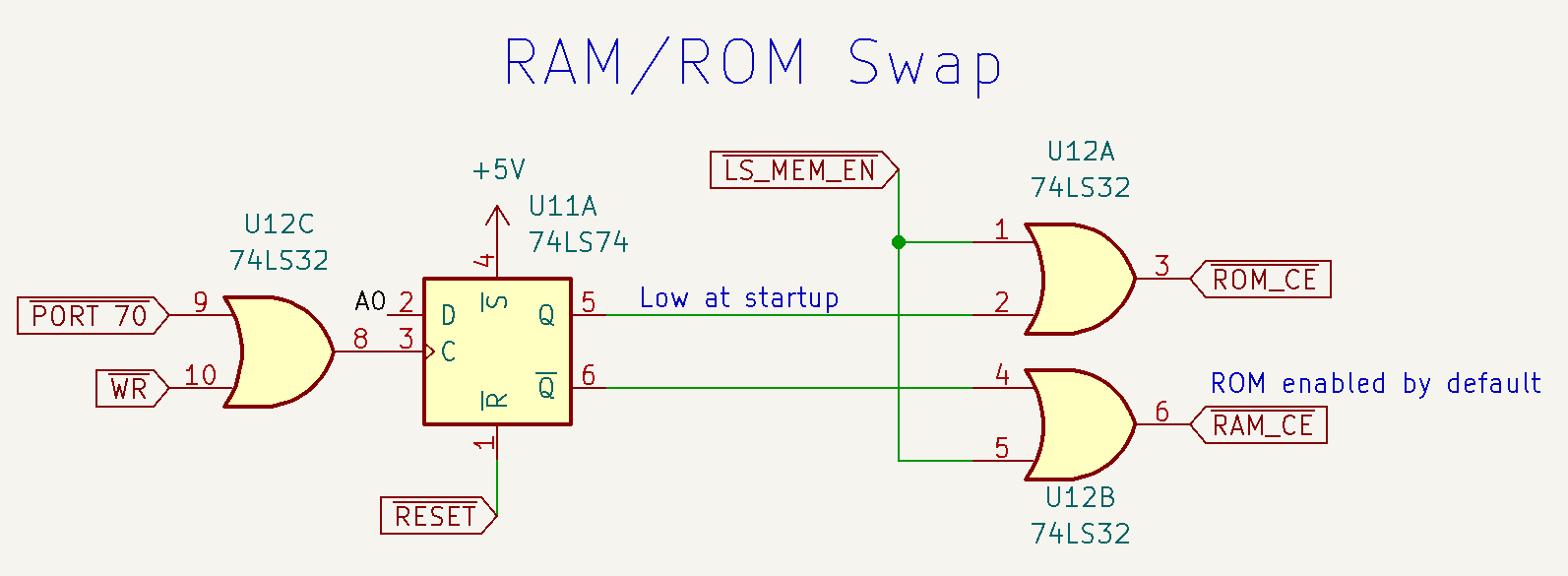
When the system starts up the flip-flop is pre-set such that the ROM is selected by default. When the system wants to swap the ROM for RAM it just simply writes 0x01 to port 70, to swap back it can simply write 0x00 to the same port.
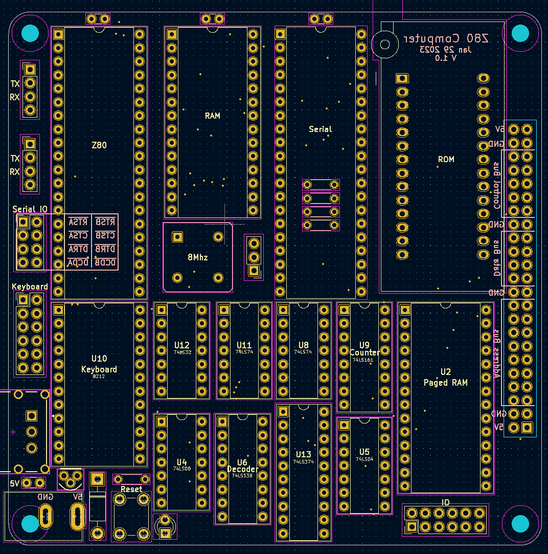
PCB
Designs And Software
You can find the newest design and plans on my GitHub page.
 ashlin4010
Comments